Altium Place Pad In Schematic
How to import designs from pads to altium designer Altium designer 15.1 Altium via pad designer
Working with a Net Label Object on a Schematic Sheet in Altium Designer
Altium module Altium via pad designer Altium wire place
Altium place wire inconsistencies
Working with a net label object on a schematic sheet in altium designerLibrary altium schematic pcb designer Pad and via templates with altium designerAdding test-points.
Altium label schematic designer documentation object working sheet electrically identify connect points labels differentAltium import Pcb design coursePcb altium schematic schema outline control creare uno databases improves convert.

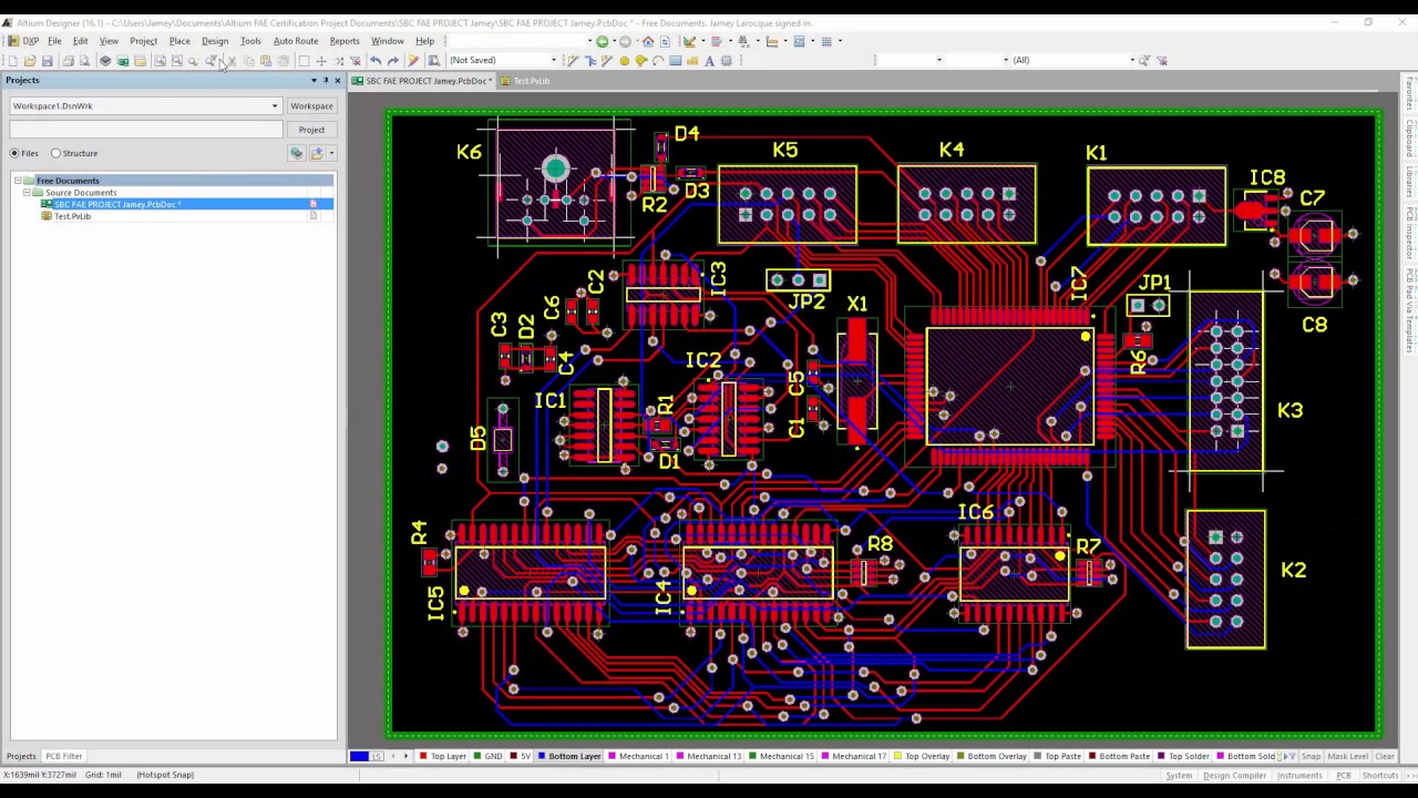
How to create a pcb layout from a pcb schematic in altium designer
.
.

Altium Place Wire Inconsistencies - YouTube

How to Import Designs from PADS to Altium Designer - YouTube
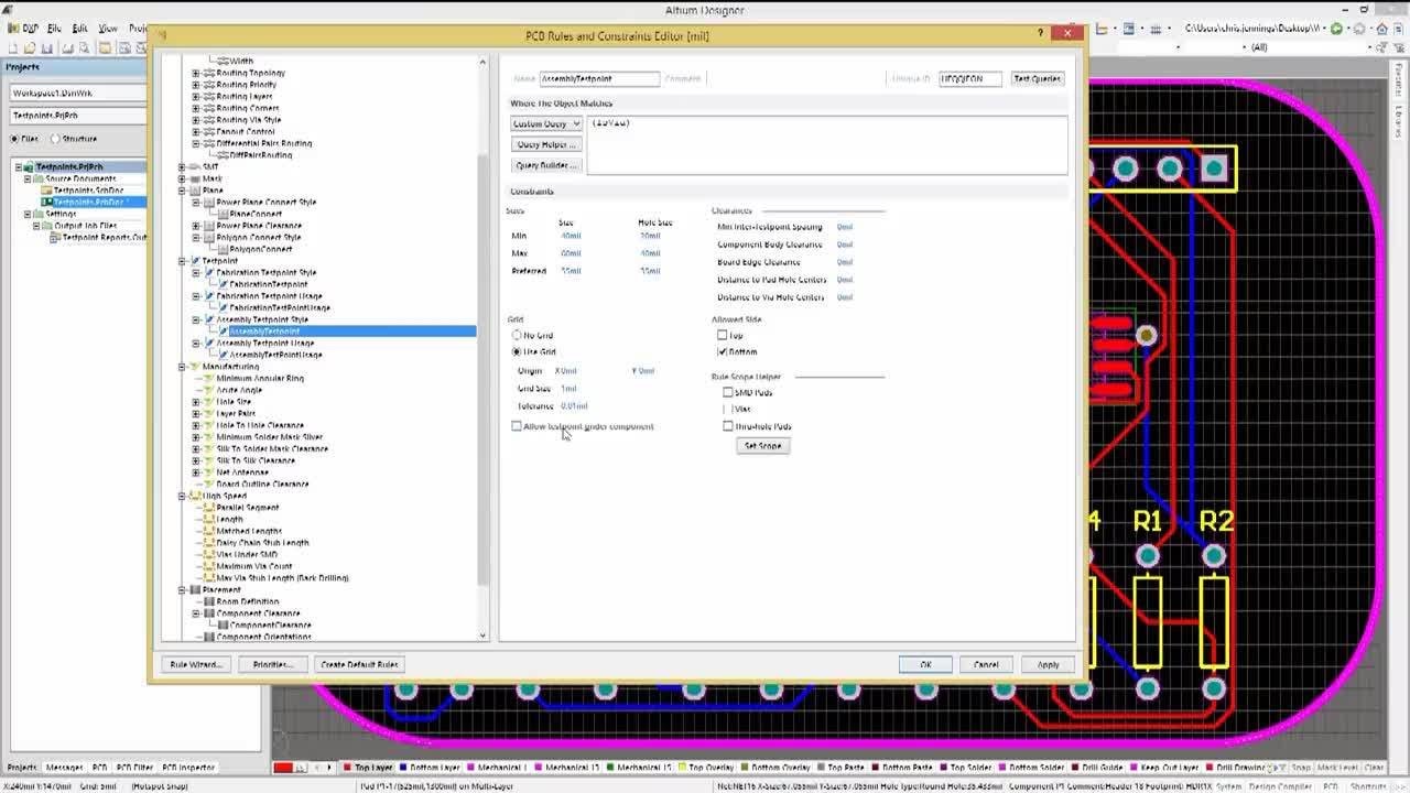
Adding Test-points | Altium Designer 17 Advanced | Module 16 - YouTube

PCB Design Course - How to make Altium Designer Schematics Library

Working with a Net Label Object on a Schematic Sheet in Altium Designer

Altium Designer 15.1 - Pad & Via Libraries - YouTube